Last Updated on November 3, 2023 by Team Yantra
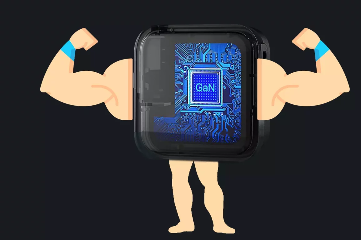
When is the last time you got excited about the chargers? I know you don’t have an answer. Well, then you should get excited about GaN chargers.
Why does it matter? What if your charger can become much smaller, much faster in charging and universal as well (one charger for multiple devices)?
Sounds cool, right? Chargers are now becoming inseparable parts of our life. The thought of our chargers becoming more compact, fast and universal for all our devices seems something to get excited about.
Introducing GaN chargers. Let’s dive into all about GaN chargers.
What is a GaN charger?
GaN charger is a charger which uses GaN based semiconductor components instead of silicon (Si) to charge your electrical devices.
GaN stands for Gallium Nitride.
Generally, Silicon is the preferred material for making transistors which are used in chargers. But the GaN charger uses Transistors based on GaN. Thus called GaN chargers.
Both GaN and Silicon, along with some other materials like Boron, Germanium, are part of a special group of material known as semiconductors. Before understanding the difference between GaN based chargers and silicon chargers. We need to know what are semiconductors.
What are semiconductors, How they are related to electronics?
Semiconductors are material who are neither completely conductors nor insulators. Their conductivity can be altered by introducing impurities in them (this process is called doping). Thus, they are called Semi-conductors as they conduct semi, not fully.
Semiconductors have properties, such as
- They can pass the current more easily in one direction than the other,
- they can have variable resistance,
- sensitivity to light or heat.
These properties are what make semiconductors like Silicon (Si) and Gallium Nitride(GaN) perfect for use in electronics.
Photo by Shawn Stutzman from Pexels
Some terminologies related to Semiconductors
Semiconductors are defined by their unique behavior of electric conductivity. They are somewhere in between insulators and conductors.
Now, these insulators, semiconductors and conductors vary from each other in terms of band gap.
You already know, everything is made up of atoms. Atoms have neutrons, protons, and electrons inside them. With, Electrons orbiting or revolving around the nucleus of the atom.
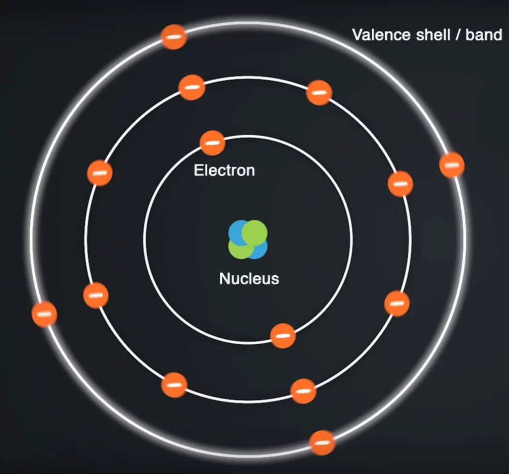
The orbits or curved path of electrons are grouped into energy levels called shells and the outermost shell is called Valence shell. Since this Valence shell represents different bands of energy levels. Therefore, also known as Valence band.
What is Valence Shell or Valence Band?
The electrons in this valence band are called valence electrons.
These electrons when gain enough energy from an external source can escape from the valence band and move to the conduction band.
Now conduction band is a band of energy levels located in the atom where electrons are free to move; thus it is called conduction band
Now, electrons move from the valence band to the conduction band.
The amount of energy required by an electron to move from the valence band to the conduction band is called the band gap
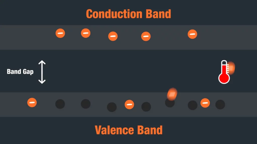
The band gap is measured in eV. The band gap varies in insulators, conductors, and semiconductors.
If the band gap is big, electrons will have a hard time jumping to the conduction band, which is the reason of the material’s poor conductivity.
| Material | Band gap |
|---|---|
| Insulators | High Band gap |
| Semiconductors | Small band gap compared to insulators |
| Conductors | No band gap, valence, and conduction band overlap |
What is GaN?
GaN stands for Gallium Nitride. It is a type of semiconductor, just like Silicon.
Gallium Nitride is a human synthesized material, made by combination of Gallium and Nitrogen. It was first synthesized around 1940s.
The first common use of GaN in electronics was in Blue LED’s in the 1990s. Before that, there were no blue LEDs, just red and green LEDs were there.
The team which made blue LEDs also received the Nobel Prize for use of GaN to make Blue LEDs possible.
GaN is also used in making Chargers (as we’re discussing here), Solar panels, radars and finding many applications in various modern electronics.
Now what makes GaN based charger better than our typical Silicon-based chargers.
What is a GaN charger?
Chargers which make use of Gallium Nitride, or GaN, based components inside them can be called GaN chargers.
One of the main component of a charger is a Power IC which is a transistor. In GaN based chargers , this power IC is made up of GaN ( Gallium Nitride. ) and in conventional chargers this chip is based on silicon.
Use of GaN based IC makes charger – provide higher power output, overall more efficient, handle higher voltages than traditional silicon-based semiconductors. The result is a smaller, lighter charger that produces less heat and offers faster charging times.
Why is GaN based charger better than Silicon-based charger?
In simple terms,
- Efficiency – GaN is much more efficient than silicon in conducting current.
- High Voltage – can withstand much higher voltages
- High Temperature – withstand higher temperatures, compared to Silicon. GaNs heat limit is 600 °C, while silicon’s is 150 °C.
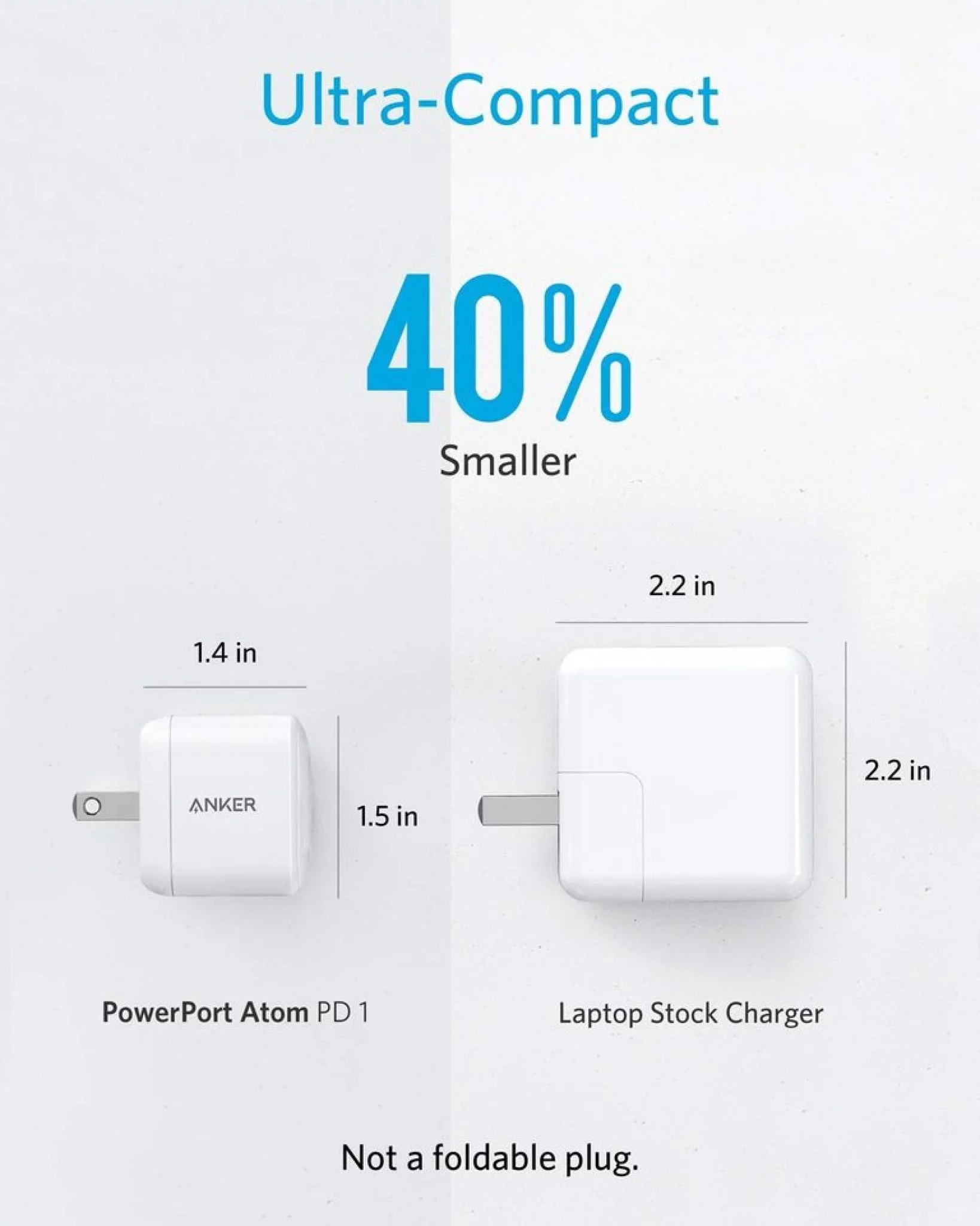
- Size – a typical GaN charger is much smaller than a silicon chip.
Now, we know that a typical charger has an electronic chip inside it. In this chip lie many electrical components.
The heart of this chip is what we call power Transistors. The main difference between Silicon-based charger and GaN based charger is due to this transistor only.
The Silicon-based charger use silicon (Si) MOSFETs (Metal-Oxide-Semiconductor Field-Effect Transistors) and GaN based charger use GaN HEMTs (High-Electron-Mobility Transistors, also called GaNFET).
Now, the advantages of GaN based charger are due to this GaN HEMTs over Silicon based MOSFETS.
Diving further, the reason for GaN being better is since GaN has a wider band gap (3.4 eV) than Silicon, which has a band gap of 1.1 eV. I have already explained above what a band gap is.
The benefits that wider band gap gives are that
- It can withstand higher temperature
- GaN can operate at higher frequencies
Additionally, GaN has more electron mobility of 2000 cm2/Vs compared to Silicon with 1500 cm2/Vs. Electron mobility is how fast electrons can travel. Thus, GaN has 30% more electron mobility than Silicon.
This higher electron mobility gives GaN the advantage of faster switching speeds. GaN has more switching frequency than Silicon based MOSFETS. Due to this, even the components which are connected to the transistor can be made smaller.
Comparison Between Properties of Silicon and GaN
| Property | GaN | Silicon | Advantage it gives | Practical Usage |
|---|---|---|---|---|
| Band Gap | 3.4 eV | 1.1 eV | Wider Band gap means , GaN can work in higher voltages and temperatures easily | GaN based products can be used for High voltage and current applications. |
| Electron mobility | 2000 cm2/Vs | 1500 cm2/Vs | Electron move faster, GaN. As a result, frequency of switching can be much higher. | Due to faster switching, the components used beside GaN transistors can be smaller. Making overall size of chip smaller. |
| Max temperature | 600 °C | 150 °C | Can easily work in High temperatures | The components can be more tightly packed without worrying about the high temperatures it generates. Increasing the overall efficiency as well. |
A GaN charger will be more efficient, have more power, and will be much smaller than a similarly rated Silicon charger.
All these properties are what makes
- Charger based on GaN more efficient than Silicon-based charger. GaN based charge has 95% efficiency compared to Silicon with 85%
- GaN charger is approximately 40% smaller than Silicon-based charger.
- Due to more power limit, GaN can simultaneously charge multiple devices. Also, thanks to USB-C, Everything is now USB-C compatible. With USB-C PD reaching 100W. We can simply have universal GaN chargers that can charge our mobile laptops etc. simultaneously.
GaN is helping chargers become faster and smaller. With some chargers being able to charge the phone fully in 8 mins only.
In fact, the mini flash chargers by Oppo makes use of this GaN technology only.
This begs the question then why we were not using GaN earlier. Let explore that.
Why was then GaN not used then in electronics until recently?
When compared to Silicon, the GaN based components are new to the market. As, for any new thing, it takes time for the mass market adaptation.
The silicon-based chips have been in uses since 1970 and are now very mature technology. They have huge industry support. They are scalable and cost-effective.
But, GaN based components became focus of researchers only after 1990s. As then, Gallium Nitride was first used for making Blue LEDs.
Silicon-based MOSFET devices have been serving the industry successfully. They are the current industry standard for power switches in power applications.
But as the technology is moving so fast. We are now reaching theoretical limits of improvements in Silicon based MOSFET devices. That is why GaN devices are becoming more and more attractive.
Besides this, two of the main problems with the GaN have been just about resolved. The problems were,
- Defects in GaN crystals
- Making GaN components in a cost-effective way
Growing GaN crystals can be very challenging. It can have many defects. The defects in silicon per 1 cm square are less than 100 while in that of gallium were more than a million.
Additionally, Since the Silicon manufacturing technology is already being used for long time. Making Silicon devices is much more cost-efficient than newer GaN.
But thanks to continued research and development on GaN materials. Now the defects in Gallium have come down to the range of 100 to 1000.
Besides, GaN based transistor can now be produced using existing machinery and processes already used to make Silicon MOSFETs.
The technique involves growing a thin layer of GaN on the AIN (Alumium Nitride) layer of a standard silicon wafer. Using metal organic chemical vapor deposition (MOCVD). This new technique of making GaNFETs was first used in 2006.
Also, adding to the fact, GaN Transitions of less than 500V do not even require much packaging as Silicon Transistors. Giving packaging advantage and reducing cost.
The reduced defects, use of existing techniques/machinery and packaging have all made GaN transistors much more viable and cost-effective.
Where can you Buy GaN chargers?
As with every new technology trend. Plenty of startups and manufacturers are getting on this GaN train. Which is a great thing.
But, some will try to take advantage of this situation as well. They will sell inferior chargers in name of GaN chargers. So, you have to be careful when buying a GaN charger.
Tips for buying GaN chargers
- When buying, You should prefer that cable is included with the charger. As, any normal cable will not be able to support the high-power charger and your device will ultimately charge slowly only.
- The length of the cable should be long enough. Small cables are not that useful.
- Also, see the length of prongs, as short length of prongs will lead to the charger getting disconnected often.
- Do check the warranty type and duration. You may not want to spend $50 on a charger without any or useless warranty.
- If you’re going with 100W charger. Know about true 100w GaN charger. Keep in mind, not all chargers which advertise 100W are actually 100W. You have to see whether the power from single USB-C port is 100W or not. Some chargers say 100W as some of 2 poets which one port supporting max 65W only and other 35W. They advertise as sum of those two (35 + 65 = 100W)
- Check the reviews of the other customers.
There are mostly two variants available in market currently. 65W and 100W.
- TECKNET 65W PD 3.0 GaN Charger –
- One of the best 65W GaN available. Comes with 1-Year warranty
- Price – $26 to $30
- Buy from Amazon- https://amzn.to/3xbZjrO
- WOTOBEUS 130W GaN Charger –
- It is a true 100W charger. Can give 100W power from a single USB-C port.
- Price – $70 to $80
- Buy From Amazon – https://amzn.to/3Aderaa
- Nekteck 100W USB-C Charger
- One of the affordable true 100W charger
- Only has 1 single USB-C port
- Price $27 to $35
- Buy from Amazon – https://amzn.to/3qFehnz
Now you even know from where you can buy GaN chargers. But what lies ahead for GaN chargers.
Future of GaN Chargers
GaN technology has come a long way. GaN technology has paved the way for much smaller and efficient electronics. In fact, if GaN could help reduce global energy consumption by almost 20% if it is used in place of silicon-based components.
GaN chargers have made chargers much smaller, faster and efficient. Going forward, we will see more and more GaN based chargers.
GaN chargers seem like a great boon to us all.
In addition, USB-C PD along with GaN chargers have made a possibility real – One charger for all devices. As more and more devices are coming with USB-C ports and GaN chargers becoming more powerful.
Has the time come for GaN chargers?
Yes, in fact, more and more main stream companies like Apple, Samsung have launched or launching their own GaN chargers.
Of course, we will keep you updated on all that. Be sure to follow Yantragyan on our social handles.
Leave a Reply
You must be logged in to post a comment.