
Last Updated on June 21, 2023 by Team Yantra
On the 16th of June, TSMC, the leading semiconductor wafer chip manufacturer, launched the North American field of the 2022 TSMC Technology Seminar.
There were some important updates on the TSMC’s upcoming plans.
- 3 nm chips will enter mass production in 2022 and available in consumer market in 2023
- 2 nm chips will enter production in 2025
- TSMC will increase production capacity of mature nodes by 50% within three years
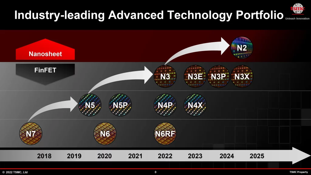
We can already see from the above roadmap shared by TSMC. The 3 nm variants of the chips will be there from 2022 to 2025 around 2.5 years, and for 2 nm it will be even more. Three-year time is substantially bigger timeline than previous timelines of say N7 or N5 nodes.
This is because as the size gets smaller, the fabrication process becomes more complex and difficult. Due to this, companies spend more time on research and development of next generation.
TSMC N3, N3E, N3P, N3X and more
To start off, N3 node will be FinFet based. Moreover, The 3 nm class of chips will have around 5 variants.
N3
Starting with N3 which is the latest upcoming semiconductor chips from TSMC. The N3 volume production as stated by TSMC will start later this year.
The N3 node is the first variant of the 3 nm class. The new 3 nm N3 will offer 10-15% performance better performance and 25-30% reduced power consumption compared to N5 (5 nm class) at same power and complexity.
But, this variant has narrow process window (these are the parameters which chip should fulfill to be qualified as valid). Due to narrow process window, the yield of the product will also be affected.
Therefore, N3 is Mostly aimed at early adopters like Apple etc. Which can pay premium for hands on the latest node and in turn benefit from the increased performance and reduced power.
N3E
The next variant of 3 nm class will be N3E. The variant will again be based on again 3 nm, but will have additional changes and improvements.
N3E will offer enhanced performance, lower power consumption, and increases the process window, which results in higher yields. Only small downside compared to N3 will slightly less logic density.
N3P, N3X and N3S
The constant enhancements over 3 nm node then leads us to N3P, N3X and N3S. Each of these variant has one main feature.
- N3P – the performance enhanced version 3 nm node
- N3S – the density enhanced version
- N3X – the ultra-high performance without caring about the power consumption
Moreover, the N3X seems like a direct successor to N4X(4 nm class). TSMC has states that it will support high drive currents and voltages.
FINFLEX Technology – Powering the N3 chips
Looking at the different variants of N3. We can see different variants specialize in different things. The TSMC FINFLEX™ technology is what enables that.
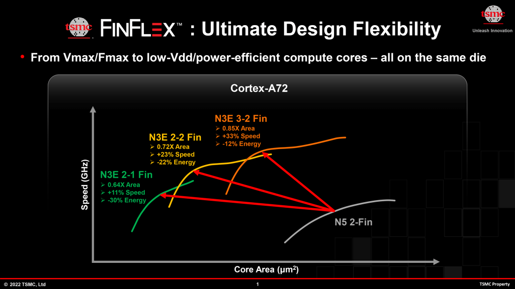
You see, a most basic building block of the chip is a transistor. This single transistor or the block is referred to as a cell.
In this case of N3, the cell of FinFet – (fin field-effect transistor) type. Now, this FinFet transistor cells make use of fins like structure for their functionality.
Now, chip designers utilize this different configurations of Fin designs for getting desired features from their chip.
For example, CPU cores in chips can be designed using 3-2 fin blocks configuration to make them run faster, or 2-1 fin standard cells to reduce their power consumption and footprint.
Thus, the different implementations lead to different pros and cons. But, when we talk about new generations of nodes like 3 nm in this case. Due to their high complexity and cost. The chip designers cannot afford to use different chips for different cases.
Thus, comes the FinFlex technology in the play. FinFlex technology offers the flexibility to mix – match the different configurations of Fin.
Like choices of different standard cells with a 3-2 fin configuration for ultra performance, a 2-1 fin configuration for best power efficiency and transistor density, and a 2-2 fin configuration providing a balance between the two for Efficient Performance.
With TSMC FINFLEX™ Chip architecture or customers can create system-on-chip designs precisely tuned for their needs with functional blocks implementing the best optimized fin configuration for the desired performance, power and area target, and integrated on the same chip.
FinFet based FinFlex technology just makes the 3 nm process from TSMC much more competitive, when compared to GAAFET/Nanosheet technology.
In all, 3 nm node from TSMC looks like another success, thanks to innovative FinFlex technology. The first batch of N3 chips will enter production later this year and arrive to the market in early 2023.
Leave a Reply
You must be logged in to post a comment.