Last Updated on July 30, 2023 by Team Yantra
Say thank you to “UFS” for making your smartphones faster and better by improving storage technology.
The storage of information and data forms the foundation of the digital world we live in today. New technology advancements have sought faster, smaller, and more efficient ways to store and access data.
One such advancement that has brought significant progress in storage technology is Universal Flash Storage (UFS).
Let’s dive deep into Universal Flash Storage (UFS), from its origin to its latest version and more.
The Basics – Memory, Flash Memory, NAND/NOR
Before we dive into the UFS storage interface, it’s important to understand some basics, such as memory, flash memory, and NAND/NOR Flash memory.
What is Memory?
In the context of computing, memory refers to the devices or systems that store information or data. Now, memories can be of two types.
- Volatile (they lose data when the power is switched off) or
- Non-volatile (they retain data even when powered down).
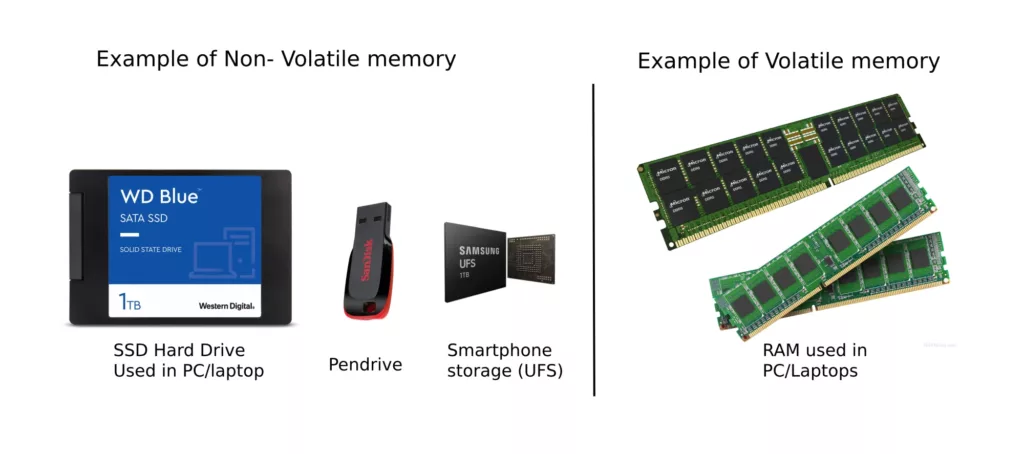
Now, for understanding UFS, we need to understand Flash memory, which is a Non-Volatile memory.
Flash Memory: A Non-Volatile memory
Flash memory is a type of non-volatile storage technology where data can be electrically erased and reprogrammed.
This form of memory is named “flash” for its ability to erase data blocks in a flash (as in speedily), much quicker than its predecessor technologies.

Image sources Ana M & Joe Chen
Flash memory was invented by Dr. Fujio Masuoka in the 1980s while working at Toshiba.
Flash memory has become a staple in our tech-driven world because of its durability, speed, and efficiency.
It’s found in many devices, from USB drives and smartphones to Solid-State Drives (SSDs) powering enterprise servers and mobile systems.
Flash memory, invented in the 1980s, has been a cornerstone of data storage, evolving through NOR and NAND types.
Flash Memory Types: NOR and NAND
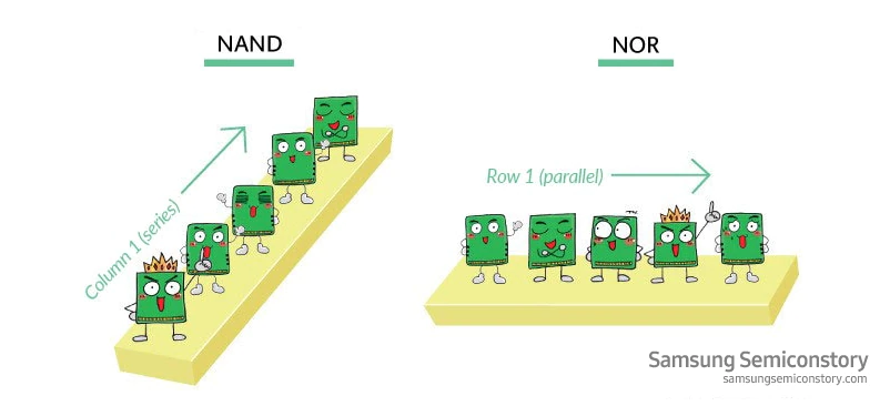
Now, Flash memory primarily comes in two forms – NOR and NAND – named for the logic gates (refers to arrangement of blocks inside flash memory) they resemble.
While both types can retain data without power and are non-volatile, they serve different purposes due to their distinct architectures.
1. NAND Flash
It is the most common type of Flash memory, used in our devices and accessories like smartphones, laptops, USB drives, Solid-State Drives (SSDs), and memory cards.
NAND flash, commercially unveiled by Toshiba in 1989, provides sequential access to data and is better for larger data files.
It’s similar to reading a book from cover to cover, where you read the data sequentially.
Because of its structure, it’s faster and more durable, and therefore ideal for storing large amounts of data.
2. NOR Flash
NOR flash, commercially introduced by Intel in 1988, allows for random access, meaning any byte in the memory can be accessed individually and is better suited for small data sizes.
It’s similar to navigating through the chapters of a book, where you can jump to any chapter directly without reading the previous ones.
Due to its structure, NOR flash offers fast random access to individual memory cells, making it suitable for executing code directly from the memory.
It is commonly used in applications such as firmware storage in microcontrollers, BIOS chips in computers, and read-only memory (ROM) for booting up systems.
Choosing NAND Flash Memory over NOR Flash memory – The Building Block of Flash Storage
While both NAND Flash and NOR Flash are used for storing data. They both have differences in how they store data. Due to which one preferred over another depending on the use case.
NOR flash stores data parallelly row wise in a horizontal arrangement. This means the memory cells align horizontally.
Whereas NAND flash is vertical. The memory cells align vertically, which makes mass storage possible in a small space by stacking the cells. Also, in NAND flash data is located order wise which makes Data reading fast on NAND.
Thus, it is easier to increase the storage capacity of NAND flash and is faster in writing data, while NOR flash is better at reading data faster.
Coming to modern-day devices like Laptops and smartphones, NAND Flash is preferred because of:
- Size and Density: NAND flash can hold more data than NOR flash of the same size, making it more cost-effective.
- Speed: While NOR flash is faster for reading individual bytes, NAND is faster at reading and writing large blocks of data.
- Durability: NAND flash is designed for high read-write endurance, making it more durable over time.
This makes NAND flash the most commonly used Flash memory type. Your current devices like smartphones, SSDs, tablets, and USB drives etc. are using Flash memory.
Now, NAND Flash memory can be further categorized based on two types –
The First is based on internal memory arrangement or data density, second how they are managed,
1. NAND Flash Memory Cell Types (Data Density): refers to the number of bits stored in each memory cell.
- SLC (Single-Level Cell): Stores 1 bit per cell. – Low storage but high Reliability
- MLC (Multi-Level Cell): Stores 2 bits per cell.
- TLC (Triple-Level Cell): Stores 3 bits per cell.
- QLC (Quad-Level Cell): Stores 4 bits per cell.
- 3D NAND (Vertical NAND) – Stores bits vertically – One stack above another. This is the most preferred choice these days.
2. NAND Flash Memory (Management Types): This category refers to how the flash memory and its operations are managed, including reading, writing, and erasing data.
- Raw NAND Flash: Memory that is accessed and controlled directly by the device’s main processor. It requires manual management for tasks like wear-leveling and error correction. Raw NAND can use any of the cell types (SLC, MLC, TLC, QLC), depending on the application’s requirements.
- Managed NAND Flash: Memory that includes a built-in controller to manage operations, freeing up the device’s main processor. Managed NAND also can use any of the cell types (SLC, MLC, TLC, QLC and 3D NAND or V-NAND), depending on the application’s requirements. Examples of managed NAND include:
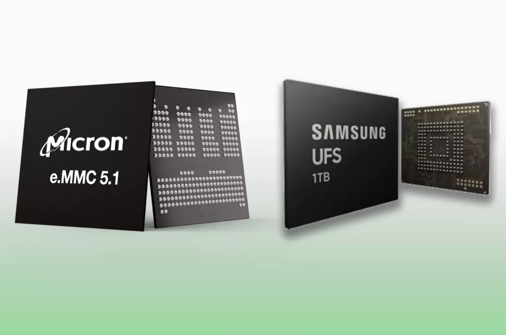
- eMMC (embedded MultiMediaCard)
- SSDs like NVMe (Non-Volatile Memory Express)
- UFS (Universal Flash Storage)
Now, the memory chips used in our smartphones and laptops are of the managed NAND Flash type. These are eMMC, UFS (which we are exploring in this article) and SSDs.
Managed NAND – From NAND Flash to Storage: eMMC and UFS.
We now know that Flash memory in our devices isn’t just bare NAND flash, it’s often packaged in standardized forms as Managed NAND Flash memory. Such as eMMC (embedded MultiMedia Card) or UFS (Universal Flash Storage).
Let’s dive further into them.
1. eMMC
eMMC is a type of flash storage commonly found in low-cost smartphones, tablets, and low-cost laptops. It combines NAND flash memory and a controller in one package, simplifying the integration process for manufacturers.
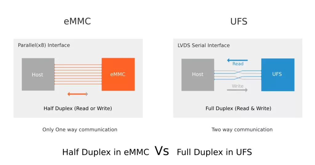
eMMC supports a wide range of data bus widths (x1, x4, and x8)However, eMMC uses a parallel interface and operates in a half-duplex manner. Meaning, it can either read or write data at a given time, but not simultaneously. This limits its speed as it can only read, write, or erase data at a time.
While eMMC has served as a reliable and cost-effective storage solution for many consumers electronic devices, including smartphones, tablets, and digital cameras, its limitations in speed and performance have led to the development of more advanced storage solutions like UFS.
2. SSDs – NVMe (Non-Volatile Memory Express):
NVMe SSDs storage is most commonly associated with PC’s, Servers and laptops. NVMe offers significantly faster data transfer rates. Thanks to its ability to handle a higher number of command queues and commands per queue.
While NVMe offers superior performance, it’s generally more costly than eMMC or UFS, and also less power efficient. Therefore, not preferred for use in mobile devices.
3. UFS
UFS is a high-performance, serial interface for flash storage. It intended to bring higher data transfer speed and increased reliability to flash memory storage while having high-power efficiency.
It was designed to be a leap forward from eMMC, addressing the demand for more substantial memory bandwidth in devices like high-end smartphones, digital cameras, and automotive applications.
UFS is a newer standard that offers significant improvements over eMMC. Its most significant advantage is that it uses an optimized serial interface, allowing it to read and write data simultaneously, significantly speeding up data transfers.
Same as eMMC, – UFS comes in two forms:
- UFS Card: A removable storage expansion, similar to a microSD card but faster.
- UFS embedded: the type that’s soldered directly onto the device’s motherboard, like eMMC.
High-level Comparison of Different Managed NAND Flash
| Criteria | NVMe | UFS | eMMC |
|---|---|---|---|
| Data Transfer | Parallel (up to 64K queues) | Serial, Scalable (multiple lanes) | Serial (1 lane) |
| Mode | Full Duplex | Full Duplex | Half Duplex |
| Speed | Very High (up to 3,500 MB/s) | High (up to 1,200 MB/s for UFS 3.1) | Moderate (up to 400 MB/s for eMMC 5.1) |
| Power | Higher power consumption | Lower than NVMe | Lowest among the three |
| Cost | More expensive | Less expensive than NVMe | Least expensive |
Looking at the above comparison, it is clear for devices like smartphones, smartwatches and tablets, where power efficiency is necessary. eMMC and UFS are the preferred choice.
eMMC and UFS are typically preferred for smartphones for the following reasons:
- Cost-Effectiveness: Both eMMC and UFS are less expensive than NVMe, making them more suitable for the cost-sensitive smartphone market.
- Power Efficiency: eMMC and UFS consume less power than NVMe, which is critical for battery-powered devices like smartphones.
- Form Factor: eMMC and UFS are designed for integration in smaller form factor devices, whereas NVMe is often used in larger form factor SSDs, making the former two more suitable for compact devices like smartphones.
Now, we have two contenders that can be used in smartphones and tablets for memory storage. eMMC and UFS.
Let’s do a quick comparison between the two:
Comparison of UFS vs. eMMC
UFS and eMMC are both preferred over NVMe in applications where low power and cost are a factor. But they both have differences, and UFS is the better choice for most applications.
One of the main points of difference is the mode of communication. eMMC module communicate over Half Duplex method whereas in UFS data is transferred in Full Duplex mode.
Half Duplex in eMMC Vs Full Duplex in UFS
| Criteria | UFS | eMMC |
|---|---|---|
| Mode | Full Duplex | Half Duplex |
| Speed | High (up to 1,200 MB/s for UFS 3.1) | Moderate (up to 400 MB/s for eMMC 5.1) |
| Command Queue | Yes | No |
| Power | Higher than eMMC, but optimized | Lower, but less optimized |
| Scalability | Scalable (up to 2 lanes) | Not Scalable (1 lane only) |
UFS is generally preferred over eMMC due to the following reasons:
- Speed: UFS offers significantly higher data transfer speeds compared to eMMC.
- Mode of Operation: UFS operates in full-duplex mode, allowing it to read and write data simultaneously. In contrast, eMMC operates in half-duplex mode, where it can either read or write at any given time.
- Command Queue: UFS has a Command Queue feature, which allows for prioritizing and optimizing tasks, thereby improving performance. This feature is absent in eMMC.
- Scalability: UFS supports multiple lanes of data transmission, allowing for further scalability. eMMC, on the other hand, is limited to a single data lane.
These factors make a UFS a better choice for use in mobile devices like smartphones and tablets for high-performance and efficient data storage.
With this understanding of managed NAND flash types and why UFS is best suited for use in smartphones. We can now dive further into the specifics of UFS memory,
Universal Flash Storage (UFS): The Evolution of Flash Memory
The Need for UFS
Before UFS, embedded MultiMedia Card (eMMC) was the primary storage device in smartphones and tablets.
As technology progressed, the demand for faster and more reliable storage emerged
However, eMMC’s interface was based on an 8-Bit parallel bus, which was holding back scaling of eMMC performance.
Thus, the storage industry started seeking better options. UFS!
The year was 2008, multiple organizations were looking for better storage options for smartphones. In the forefront were:
- JEDEC (Joint Electron Device Engineering Council) Solid-State Technology Association and
- MIPI (Mobile Industry Processor Interface) Alliance.
JEDEC association previously set the eMMC standard, but now, they were looking better alternative as eMMC was already hitting its limits due to the emergence of newer and better smartphones.
JEDEC was looking at serial interfaces as a means for future storage requirements.
Parallelly, the (MIPI) Alliance was working on its own high-performance specifications to enable chip-to-chip data communication for cameras, latest media devices and display interfaces.
In 2010, JEDEC collaborated with the MIPI Alliance, and in 2011, the Universal Flash Storage (UFS) standard was announced and published.
In 2010 only, a new organization was formed, the Universal Flash Storage Association (UFSA), with the aim to develop an ecosystem and support environment for UFS devices and host applications.
Then in June 2011, UFSA published a UFS white paper.
UFS was designed as a high-performance, low-power storage standard to bring higher data transfer speed and increased reliability to flash memory storage.
The initial version of UFS was UFS v1. Since then, there have been more updates to the standard, with v4 being the latest version for embedded UFS.
Toshiba (Now Kioxia) was the first company to announce and support UFS chipset bases on UFS v1.1.
What is UFS memory?
UFS, or Universal Flash Storage, is a high-performance memory storage/interface. UFS is specially designed for devices or applications where high performance is needed, but power consumption needs to be minimized, like smartphones, digital cameras, and other devices.
The UFS standard was first defined by the JEDEC Solid-State Technology Association, an independent semiconductor engineering trade organization.
The project began around 2007 with the goal of revolutionizing the existing memory storage landscape and making a significant leap from the limitations of previous technologies such as eMMC (embedded MultiMedia Card) and microSD.
The UFS storage interface offers high-speed read-write performance. Which is crucial in today’s high-end electronic devices such as smartphones, digital cameras, and tablets.
Technical Aspects of UFS: How UFS works and its Architecture
Universal Flash Storage works by using a combination of hardware and software to store and retrieve data on NAND flash memory chips. Below is the high-level overview of the UFS system inside a typical smartphone.
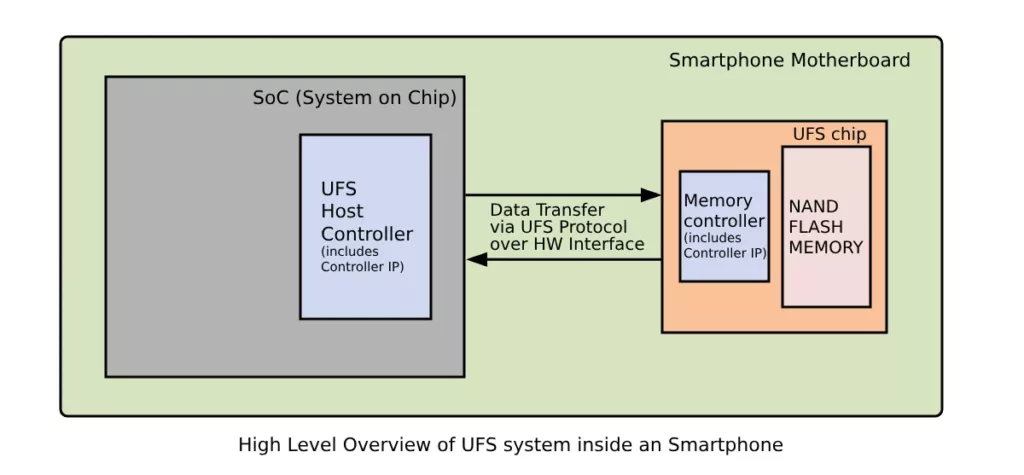
At one end we have the SoC of the smartphone and on the other end we have UFS memory chip.
SoC – System the on Chip (SoC) in your smartphone is essentially the brain of the device. CPU, GPU, etc. are all part of the SoC. The SoC has the main processing unit and the UFS host controller.
The UFS host controller’s primary task is to convert data received from the processing unit into a UFS-compliant format.
Data is then transferred from the SoC over to the UFS memory chip, which stores all the data of the device.
The data communication between the SoC and UFS memory chip happens via a specialized hardware interface, guided by the UFS protocol.
The UFS chip has a memory controller which is part of the UFS device controller. This part essentially takes data and controls the data flow to the NAND Flash, which is where actual data resides.
This high-level overview gives us the basics of the UFS system. But there is more to UFS for which we need to deep dive further.
To understand further the working of UFS. Let’s take a look at the UFS interface inside your smartphone
UFS Interface
The Universal Flash storage system uses a “Host and” device” model of operation.
Here, the smartphone SoC is the host and the UFS memory chip is the device
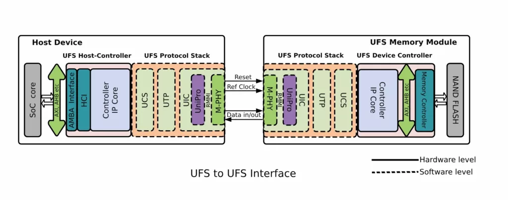
A full-fledged UFS to UFS interface has both hardware and software components.
Hardware Components
Host Side
- UFS controller host side – The UFS Host Controller is an integral component of a device that oversees the transmission of data between the SoC and the UFS memory. It comprises the AMBA Interface, the Host Controller Interface (HCI), and the Controller IP core.
- HCI – Host Controller Interface – The UFS Host Controller Interface (HCI) is an interface that enables the host system to communicate with the UFS device. It enables communication with the software components. It manages the execution of commands, interrupt signaling, and status reporting.
- Controller IP core – bridges the system with the UFS memory. It interprets high-level system commands into a format that the UFS can understand and manage. Manage all aspects of UFS communication and control, including error handling, data flow management, and interfacing with the host system.
- AMBA (Advanced Microcontroller Bus Architecture) Interface: AMBA is a standard open bus architecture designed by ARM. It’s used as the on-chip communication standard for designing high-performance system-on-chip designs. The AMBA interface in a UFS system is used to connect the UFS host controller to the host system.
- AXI (Advanced extensible Interface): – AXI is a part of the AMBA interface standard. It’s used for high-speed communication between high-performance system modules. In the context of UFS, the AXI interface can be used to connect the UFS host controller to the system processor or other high-speed components in the host system.
- AHB (Advanced High-performance Bus): – AHB, another part of the AMBA standard, is used for connecting lower latency components. Although it’s not as high-performance as AXI, it’s simpler and offers lower latency. It might be used in a UFS system for connections to lower-speed, lower-latency components.
Device side
- UFS controller – Performs same task as UFS controller on host side
- Controller IP core
- Memory Controller – manages the flow of data to and from the physical memory. It coordinates read and write operations, manages access timings, and ensures data integrity. By providing an interface between the SoC and the memory, the Memory Controller allows for the efficient management and retrieval of data, significantly improving the device’s performance.
- NAND Flash memory – the physical storage space where data is held. Characterized by its high density and non-volatile nature, it retains stored information even when power is switched off. NAND Flash Memory offers fast read, write, and erase times, making it an ideal choice for mobile devices. Its architecture supports a large number of write/erase cycles, ensuring longevity and reliable performance.
Additional components include AXI, and AHB – which facilitate communication between different components inside the chip.
Software Components
The UFS protocol is the software component of the UFS system. This set of protocols supports efficient communication between the host (SoC) and Device (the UFS memory). It’s composed of the UFS Command Layer (UCS), UFS Transport Protocol Layer (UTP), and the Interconnect Layer (UniPro + M-PHY).
By using these standard interfaces and architectures, the UFS system can efficiently and effectively manage data storage and retrieval for the host device.
UFS Protocol Architecture
The UFS architecture is made up of three major layers:
- the UFS Command Layer (UCS),
- the UFS Transport Protocol Layer (UTP), and
- the Interconnect Layer (UniPro + M-PHY).
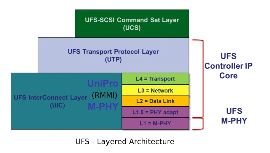
1. UFS Command Layer (UCS):
The UCS layer is responsible for handling and managing SCSI commands sent from the host. SCSI (Small Computer System Interface) is a standard set of commands used for communication between the host system and storage devices. The UFS memory system uses these SCSI commands for tasks such as data read, write, and erase operations. UCS translates these high-level commands into commands that the UFS Transport Protocol Layer can process and execute.
2. UFS Transport Protocol Layer (UTP):
The UTP layer is the middle layer in the UFS stack that connects the UCS and the Interconnect Layer. Its primary job is to package or wrap the SCSI commands coming from the UCS into UTP packets. These packets are then transferred to the Interconnect Layer.
This layer also has the functionality to support multiple command queues, allowing for simultaneous command execution and therefore higher efficiency. The multiple command queues can prioritize operations to optimize the device’s performance, a significant upgrade from previous flash storage technologies.
3. UIC UFS Interconnect – Interconnect Layer (UniPro + M-PHY):
The Interconnect Layer is actually a combination of two components: the UniPro (Unified Protocol) and the M-PHY (Mobile Physical Layer).
- The UniPro
- protocol works at the data link layer and provides reliable data transport service.
- It’s responsible for managing data flow, including segmentation, reassembly, and error handling.
- The M-PHY
- is a high-speed physical layer interface designed for mobile devices. It’s responsible for transmitting the data across the physical connection between the host and the UFS device.
- It operates in a high-speed mode for data transmission and a low-speed mode for power saving when data transmission isn’t needed.
- UniPro and M-PHY are connected via RMMI –
- The RMMI, or Register Mailbox MIPI (Mobile Industry Processor Interface), is a key element in the UniPro protocol layer used in UFS architecture.
- It provides a simplified communication method for data transfer between the host and the device, offering an efficient and reliable mechanism to manage and control the flow of information.
The combined UniPro and M-PHY layers enable high-speed, reliable data transfer between the host device and the UFS storage.
Giving you High level overview of M-Phy and UniPro.
Think of M-PHY as the “communication highway” that allows devices (Device and Host in our case) to talk to each other at high speeds, ensuring smooth data transfer.
On the other hand, UniPro acts like a “traffic controller,” managing the flow of information between different parts of the UFS storage system and making sure everything works efficiently.
By working together, these two layers provide high-performance, reliable, and efficient data storage and transfer capabilities, allowing UFS to significantly outperform previous flash storage solutions.
This multi-layered architecture of UFS allows it to handle higher data rates, perform more tasks simultaneously, and provide more reliable performance compared to previous storage solutions like eMMC.
Working of UFS – A real word Example
To consolidate our understanding, let’s consider a practical example. Suppose you’re saving a photo on your smartphone. The SoC generates the data (photo), which then passes through the hardware components (AXI/AHB, UFS Host Controller, Memory Controller), travels across the UFS Protocol Stack, and finally gets stored in the NAND Flash Memory of the UFS device.
Key Features of UFS
- Serial Interface Technology: UFS uses a high-speed serial interface that is full-duplex, meaning it can perform simultaneous read and write operations. This technology contributes to UFS’s power efficiency and performance enhancement.
- Command Queue: The UFS standard employs a command queue system that can line up tasks and execute them in the most efficient order. Similar to a Solid-State Drive (SSD), it supports multiple commands at the same time and allows simultaneous read and write operations, contributing to high-speed operations.
- Deep Sleep State: In terms of power efficiency, UFS introduces a new power-saving state called “Deep Sleep.” This feature significantly reduces power consumption when the device is idle or not in use.
- Scalability: UFS supports a wide range of storage capacities, making it suitable for various devices and applications, from smartphones to automotive applications.
- Security: To safeguard data, UFS supports several security features, including secure erase, secure trim, and hardware reset.
- Backward Compatibility: Despite its superior performance, UFS is backward compatible with eMMC and eSD hosts.
Advantages of UFS
- High-Speed Data Transfer: Thanks to its full-duplex serial interface, UFS can simultaneously perform read and write operations, leading to significantly improved data transfer rates.
- Efficient Queuing Mechanism: The ability to queue multiple commands at once enhances random read/write performance by reducing the overhead time between commands.
- Lower Power Consumption: UFS uses less power than other forms of flash memory, thanks to its low active energy and even lower sleep-mode power draw. This is especially beneficial for devices running on battery power.
- Flexibility and Multitasking: The capability to conduct concurrent data read/write operations offers better multitasking capabilities.
The Evolution of UFS: Different versions of UFS
Like all technologies, UFS has evolved, with each new version bringing enhancements and improvements.
UFS v1.0
UFS 1.0, the first iteration of the standard, was introduced in 2011, followed by UFS 2.0 in 2013, which significantly improved performance. The most recent iteration, UFS 4.0, was announced in August 2022 by JEDEC and offers even more advanced features and improvements over its predecessor.
UFS v2.0
The UFS 2.0 standard, introduced in 2013, offered a significant performance boost over its predecessor, UFS 1.1. It also introduced a feature known as Command Queue, which improved the random read/write performance by optimizing the order of data requests.
The first consumer device with UFS was the Samsung Galaxy S6 (2015), based on v2.0.
UFS 2.1
UFS 2.1, introduced in 2016, brought minor updates to UFS 2.0. It introduced features like Secure Erase and Secure Trim, which provided a method to securely delete data.
UFS 3.0
UFS 3.0, announced in 2018, doubled the data rate of UFS 2.1, reaching up to 11.6 Gbps per lane, and improved power management features. It also provided better support for automotive applications, with a wider temperature range.
UFS 3.1
The UFS 3.1, was introduced in 2020. It incorporated features like Write Booster, an SLC (Single-Level Cell) non-volatile cache, and DeepSleep, a new low-power state. These enhancements increased performance, improved power efficiency, and prolonged the lifespan of UFS storage.
Kioxia(formerly Toshiba) was the first to release UFS v3.1 in Feb 2020.
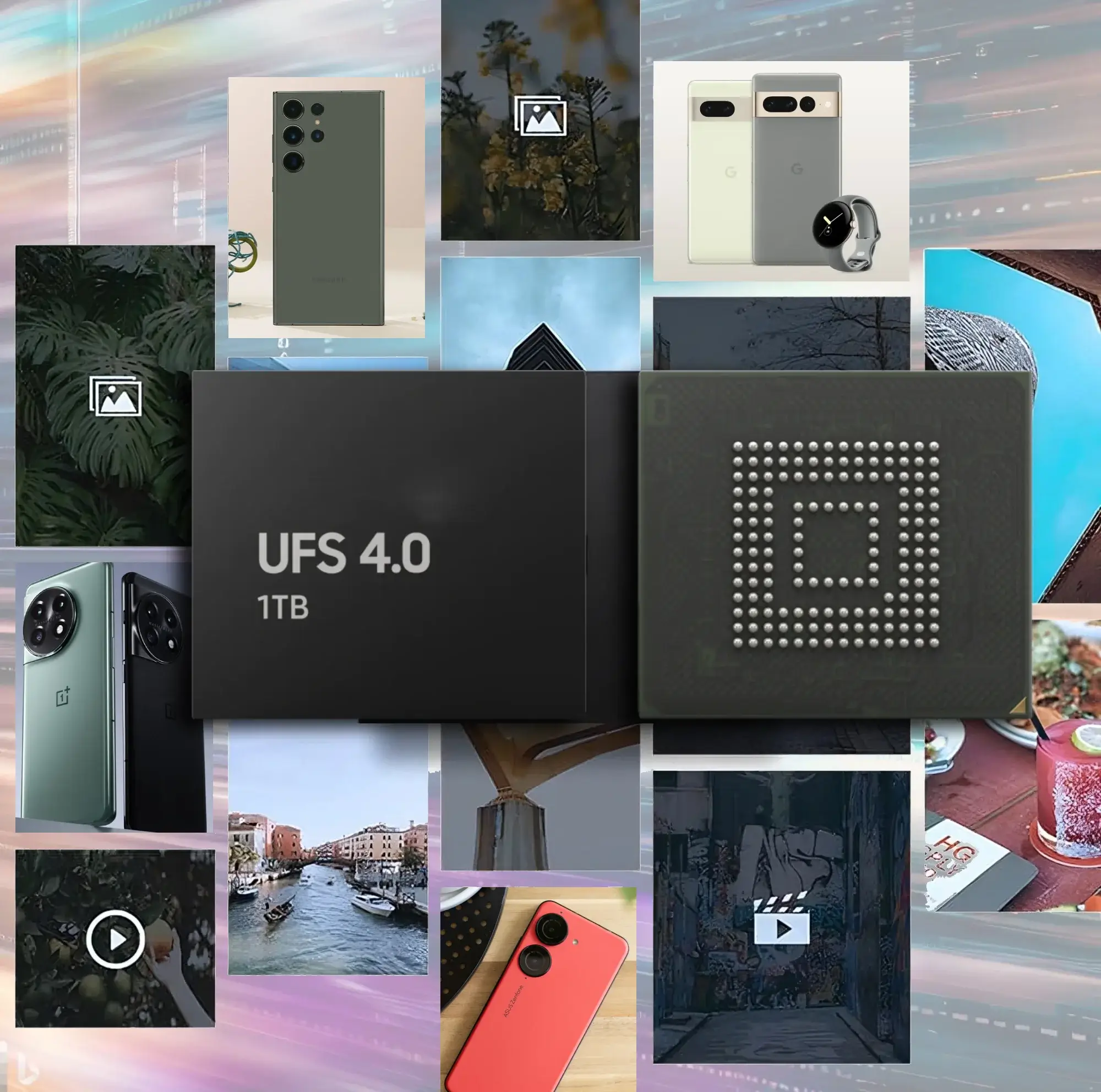
UFS 4.0
Introduced in 2022, UFS 4.0 is a transformative update to Universal Flash Storage that considerably amplifies data transfer speeds, doubling the reading and increasing the writing speed by 1.6x compared to UFS 3.1. Delivering up to 4200 MB/s read and 4000 MB/s write speeds. Samsung was the first company to launch UFS 4.0 module. Micron has also launched their UFS 4.0 chip.
You can specifically know more about UFS v4.0 in separate article.
UFS 4.0 is also 46% more power efficient, contributing to longer battery life in mobile devices. Furthermore, it strengthens data protection with enhanced Replay Protected Memory Block, making it twice as effective at shielding sensitive information.
Finally, UFS 4.0 paves the way for slimmer, denser memory chips, reducing thickness to just 1 mm while expanding storage capacity to 1 TB, thus facilitating more compact device designs.
Different UFS versions comparison
| UFS Version | Date Introduced | Sequential Read/Write Speed (MBPS) | Companies that provide UFS module for the version |
|---|---|---|---|
| 1.0 | 2011-02-24 | 300 / ? | Samsung, Toshiba |
| 1.1 | 2012-06-25 | 300 / ? | Samsung, Toshiba |
| 2.0 | 2013-09-18 | 850 / 260 | Samsung, Toshiba |
| 2.1 | 2016-04-04 | 860 / 255 | Samsung, Toshiba, Micron |
| 2.2 | 2020-08 | 860 / 255 | Samsung, Toshiba, Micron, SK Hynix |
| 3.0 | 2018-01-30 | 2100 / 410 | Samsung, Toshiba |
| 3.1 | 2020-01-30 | 2100 / 1200 | Samsung, Toshiba, SK Hynix |
| 4.0 | 2022-08-17 | 4200 / 2800 | Samsung |
UFS in Various Devices
UFS is not limited to smartphones; it finds applications in various other devices, such as
- Smartphones and Tablets
- digital cameras,
- gaming consoles,
- Automotive
- Virtual Reality (VR) and Augmented Reality (AR).
The high data transfer speed, increased reliability, and improved power efficiency make UFS a go-to choice for manufacturers aiming to enhance user experience.
Corresponding UFS version with processors and popular smartphones
| UFS Version | Processors Implemented in | Popular Devices Using This Version |
|---|---|---|
| UFS 2.0 | Snapdragon 820 and 821, Kirin 950 and 955, Exynos 7420 | Samsung Galaxy S6, Huawei Mate 8 |
| UFS 2.1 | Snapdragon 712 (710&720G), 730G, 732G, 835, 845 and 855. Kirin 960, 970 and 980. Exynos 9609, 9610, 9611, 9810 and 980 | Samsung Galaxy S9, Huawei P20 Pro |
| UFS 3.0 | Snapdragon 855, 855+, 860, 865, Exynos 9820–9825, and Kirin 990 | Samsung Galaxy S10, OnePlus 7 Pro |
| UFS 3.1 | Snapdragon 855+/860, Snapdragon 865, Snapdragon 870, Snapdragon 888, Exynos 2100, and Exynos 2200 | Samsung Galaxy S21, Xiaomi Mi 11 |
| UFS 4.0 | MediaTek Dimensity 9200 and Snapdragon 8 Gen 2 | Samsung Galaxy S23, Motorola Edge X30, Xiaomi 12 Pro |
Key Players in the UFS Market
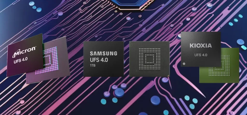
- Samsung Electronics: A leading player in the global UFS market, Samsung Electronics has made significant strides in the development and commercialization of UFS memory chips. They were one of the first to introduce UFS 2.0, 2.1, and 3.0 storage devices. Their most recent advancements have brought us the first 512 GB UFS 3.1 storage, which offers an unprecedented read speed.
- Toshiba Memory Corporation (now Kioxia): Toshiba Memory Corporation, now known as Kioxia, is another big player in the UFS market. Toshiba was one of the first companies to demo a UFS memory module based on UFS v1.1. They have been innovating and delivering competitive UFS solutions that meet the data and performance demands of contemporary digital devices.
- Micron Technology: Micron is an American multinational company that produces many forms of semiconductor devices, including UFS memory. They provide high-quality, high-speed UFS solutions tailored for a variety of applications.
- SK Hynix: This South Korean manufacturer is also prominent in the UFS market. They have a diverse portfolio of UFS memory solutions that provide high-speed, high-capacity data storage for a range of devices.
- Western Digital: A well-known name in data storage technology, Western Digital has also made their mark in the UFS memory market. Their iNAND MC EU321 UFS EFD is designed to empower mobile computing devices with enhanced capability and reliability.
These companies, among others, play a crucial role in the growth and development of UFS technology. Their innovations and advancements help drive the evolution of digital storage solutions, pushing the boundaries of speed, capacity, and performance.
The Future of UFS
The UFS landscape is poised for continuous growth, with the roadmap projecting further enhancements in performance, capacity, and power efficiency. With the demand for faster data transfer rates and higher storage capacities,
Additionally, future versions of UFS are expected to continue lowering power consumption, enabling longer device runtime and enhanced device longevity
Conclusion
In conclusion, UFS is a great technology that has significantly improved the storage capabilities of high-end electronic devices. Its speed, power efficiency, and scalability make it an excellent choice for device manufacturers. UFS is only going to me more mainstream and will be scaled further from here.
Leave a Reply
You must be logged in to post a comment.