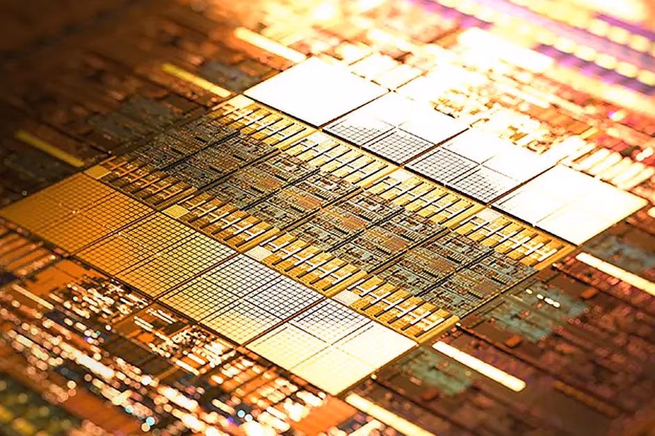
TSMC has announced significant progress in its 3nm process technology, introducing two new nodes: N3P and N3X. These developments aim to enhance performance and efficiency for a range of applications, from consumer electronics to high-performance computing (HPC).
N3P, an optical shrink of the existing N3E node, maintains design rule compatibility, allowing for seamless IP reuse. This node offers a 5% performance increase at the same leakage or a 5–10% power reduction at identical frequencies.
Additionally, it provides a 4% boost in transistor density for designs with a typical mix of logic, SRAM, and analog blocks. These improvements are achieved through refined lithographic techniques, benefiting SRAM-intensive designs in particular. N3P entered volume production in the second half of 2024, with customer product tape-outs already underway.
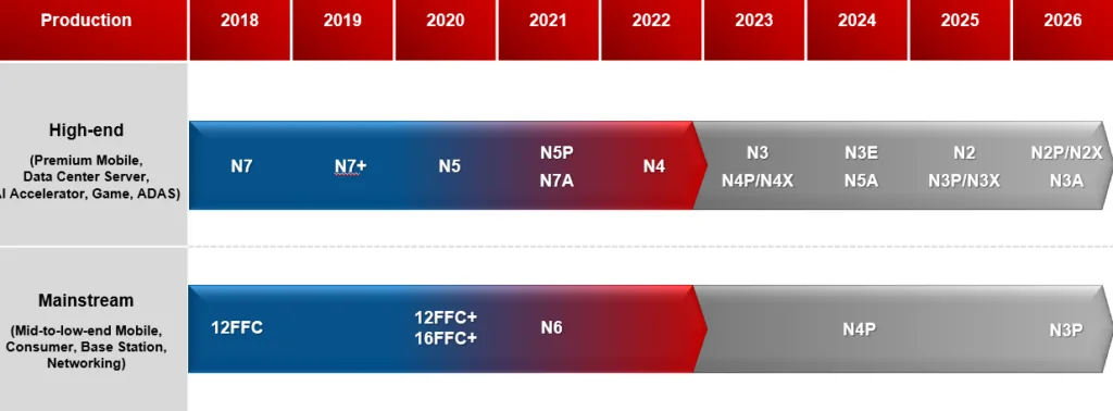
Building upon N3P, the N3X node is tailored for HPC applications such as CPUs and GPUs. It delivers a 5% performance gain over N3P and supports operating voltages up to 1.2V, which is a notable increase for 3nm-class technology.
This higher voltage enables maximum frequency (Fmax) performance but comes with a trade-off: up to 250% higher leakage power compared to N3P. Therefore, N3X is best suited for environments where power consumption is less constrained, and performance is crucial. TSMC plans to commence mass production of N3X chips in 2025.
TSMC’s roadmap includes the development of 2nm technology utilizing gate-all-around (GAA) nanosheet transistors, promising significant enhancements in performance, power efficiency, and transistor density. Production is anticipated to commence in 2025.
Source: Information sourced from TSMC’s official announcements and industry analyses.
Leave a Reply
You must be logged in to post a comment.