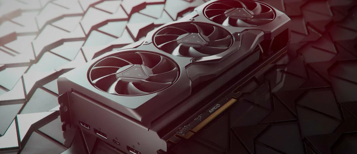
AMD has finally launched its next-generation RX 7000 series Radeon GPUs, which look impressive. After launching their Zen 4 processors a few weeks back, AMD will first launch its flagship models RX 7900XTX and RX 7900XT.
The two cards, which will hit the shelves on December 13th, will be based on RDNA 3 architecture. According to AMD, the new 7900 XTX will outperform the previous flagship, the 6950 XT, by up to 70% at 4K.
This performance boost results from several architectural improvements in RDNA that offer 54% more performance per watt than RDNA 2, as well as higher clock speeds thanks to TSMC’s 5nm (and 6nm) processes and higher overall power consumption.
RX 7900XTX and RX 7900XT specifications
| RX 7900XTX | RX 7900XT | RX 6950XT | RX 6900XT | |
|---|---|---|---|---|
| Stream Processors | 12288 | 10752 | 5120 | 5120 |
| Compute Units | 96 | 84 | 80 | 80 |
| Game Clock | 2.3 GHz | 2.0 GHz | 2.1 GHz | 2.015 GHz |
| Boost Clock | 2.5 GHz | 2.4 GHz | 2.31 GHz | 2.25 GHz |
| Memory Clock | 20 Gbps | 20 Gbps | 18 Gbps | 16 Gbps |
| VRAM | 24GB | 20GB | 16GB | 16GB |
| Memory Bus Width | 384-bit | 320-bit | 256-bit | 256-bit |
| Infinity Cache | 96MB | 80MB | 128MB | 128MB |
| Power | 355W | 300W | 335W | 300W |
| Process | GCD: TSMC 5nm MCD: TSMC 6nm | GCD: TSMC 5nm MCD: TSMC 6nm | TSMC 7nm | TSMC 7nm |
| Architecture | RDNA3 | RDNA3 | RDNA2 | RDNA2 |
| GPU | Navi 31 | Navi 31 | Navi 21 | Navi 21 |
| Launch Price | $999 | $899 | $1099 | $999 |
| Launch Date | 13 Dec 2022 | 13 Dec 2022 | 10 May 2022 | 8 Dec 2020 |
With RX 6000 series cards, while AMD has given very tough competition to Nvidia RTX 3000, AMD cut down on its prices making it much more attractive to buyers. AMD is applying a similar tactic now, pricing its flagship GPU much cheaper than RTX 4090.
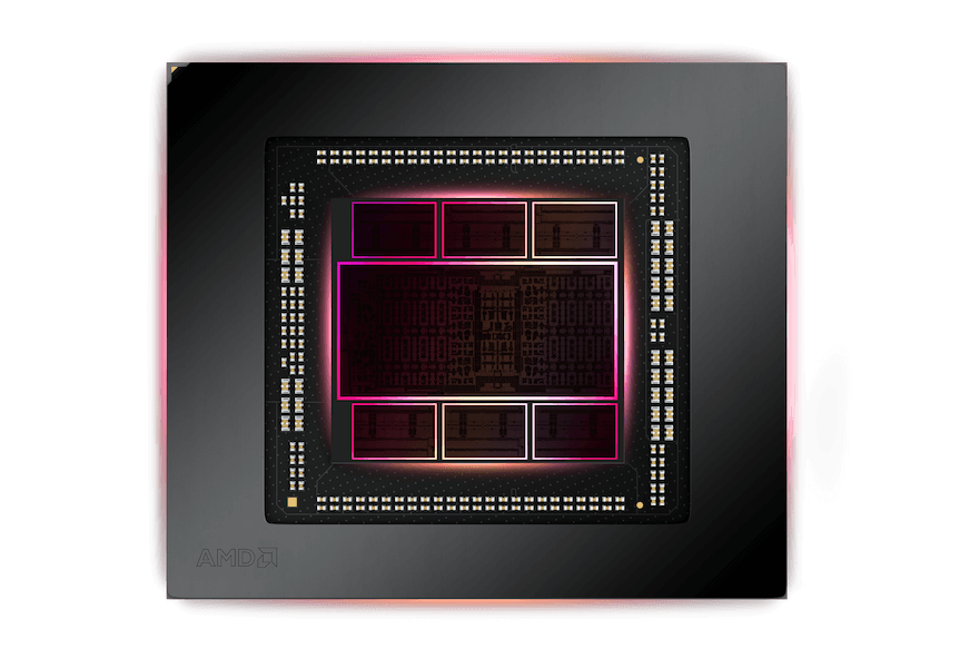
AMD will use Chiplets for its RX 7000 GPU
When AMD came up with Zen processors, it reinvented processors with Chiplet design which uses a modular approach to build processors. It uses multiple chips with different functions to form a unit of a process.
AMD is using chiplets in the construction of the GPU for the first time from any of the big three GPU manufacturers.
Chiplets are the holy grail of GPU construction in some ways because they allow GPU designers to break apart complex monolithic GPU designs into multiple smaller parts, allowing for new scaling options as well as mixing and matching the process node used in manufacturing. This improves yield and reduces cost.
However, it is also a holy grail because the enormous amount of data that must be passed between different parts of a GPU (on the order of terabytes per second) is extremely difficult to achieve – and extremely necessary if a multi-chip GPU is to present itself as a single device.
How does Chiplet design work in favour of AMD?
AMD has assembled two types of chiplets for their big Navi 31 chip, essentially breaking off the memory functions from a traditional GPU into their own chiplets. This means that the GPU’s core functions are housed in what AMD refers to as the Graphics Compute Die (GCD), which houses all of the ALU/compute hardware, graphics hardware, and ancillary blocks such as the display and media engines.
Meanwhile, AMD’s infinity cache (L3 cache) and 64-bit (technically 2×32-bit) GDDR6 memory controllers are housed on the new Memory Cache Die (MCD).
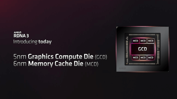
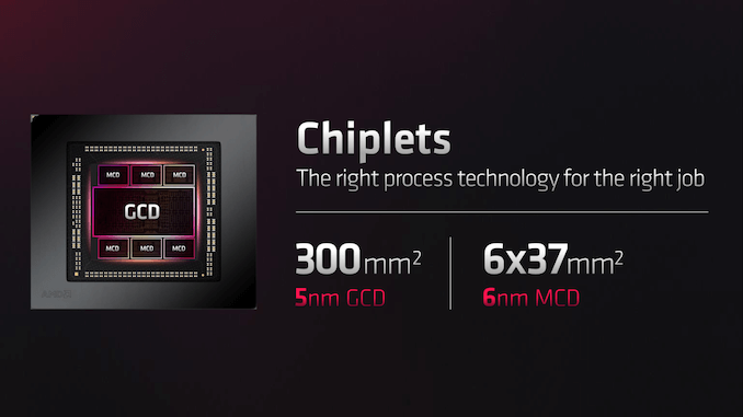
GCD houses the important performance-critical aspects of the overall GPU and is built on TSMC 5nm process. Meanwhile, AMD’s infinity cache (L3 cache) and 64-bit (technically 2×32-bit) GDDR6 memory controllers are housed on the new Memory Cache Die (MCD).
This provides AMD with the highest density, power consumption, and clock speeds for these parts, albeit at a higher manufacturing cost. The GCD die size is 300mm2.
On the other hand, the MCD is one of the chiplet’s scalable aspects, as Big Navi 3x GPU SKUs can be configured by pairing them with more or fewer MCDs.
RX 7000 performance improvement
Whereas RDNA 2’s compute core was largely unchanged from RDNA 1, RDNA 3 introduces a few significant changes.
The most significant impact is how AMD organises their ALUs. In short, AMD has doubled the number of ALUs (Stream Processors) within a CU, increasing from 64 to 128 in a single Dual Compute Unit.
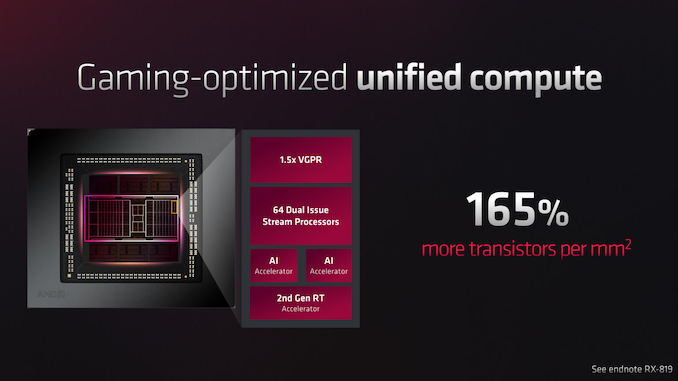
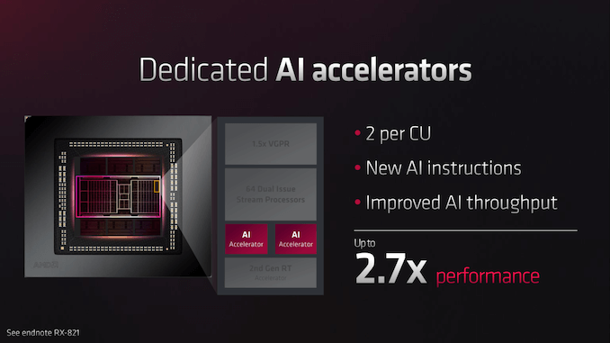
More importantly, AMD has finally integrated specialised AI processing into their consumer GPUs. This is an area where both NVIDIA and Intel have already invested in their consumer chips, and as the use of GPU inference in workloads grows, AMD cannot ignore it any longer.
Another area where AMD talked about massive improvement is the ray tracing performance and it does by integrating what they are calling second generation RT accelerator. AMD claims that it can handle 50% more ray-tracing on flight and offer 50% improved performance.
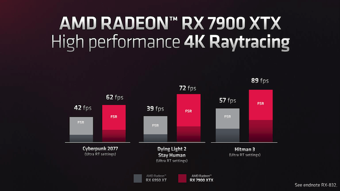
While AMD didn’t offer any helpful and real data about its performance, it did provide a vague performance increase of their RTX 7900XTX and RX7900XT over previous generation’s RX 6900XT.
AMD’s own performance slides claim a 47% to 84% boost in RT performance. It should be emphasised, however, that AMD’s figures are with FSR enabled, so we cannot separate these increases from any adjustments that improve FSR performance on the 7900 XTX.
Leave a Reply
You must be logged in to post a comment.